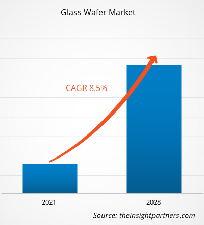
Every smartphone camera, wearable sensor and advanced chip package rests on materials most users never see. Among them, thin, flat and exceptionally clean glass is becoming indispensable, and the Glass Wafer Market is climbing from US$ 454.63 million in 2025 to a projected US$ 987.41 million by 2034. That trajectory equates to a 9.0% CAGR across 2026-2034. As semiconductor makers push for smaller, faster and more heterogeneous devices, glass wafer demand is moving from a niche need to a mainstream requirement.
What Is a Glass Wafer?
A glass wafer is a thin, precisely polished disc of glass, often borosilicate or fused silica, produced to the same dimensions as silicon wafers. Its transparency, thermal stability and electrical insulation make it valuable as a carrier, cap or substrate. Manufacturers use it for sensors, packaging and microscale devices.
Request a Sample Copy of the Report: https://www.theinsightpartners.com/sample/TIPRE00020116
What Is Driving Demand in the Glass Wafer Market?
Start with imaging. Smartphones, vehicles and security systems now carry multiple cameras, and each CMOS image sensor needs protective, optically clear glass at wafer level. As resolution rises and modules shrink, tolerances on thickness, flatness and surface quality tighten. That pressure favours specialist suppliers and supports steady growth in the glass wafer market.
Advanced packaging adds a second engine. Chipmakers are stacking, bonding and rerouting dies in new ways, and glass wafers serve as temporary carriers or permanent substrates during these steps. Compared with many alternatives, glass offers a close match to silicon’s thermal behaviour, excellent flatness and the ability to pass light for laser debonding. What makes this particularly significant is that packaging, not just transistor scaling, now decides performance gains, so glass wafer volumes rise alongside every new packaging platform.
Beyond that, MEMS, radio frequency components and microfluidic devices broaden the base. Automotive sensors, medical diagnostics and 5G front-end modules rely on hermetic sealing and low signal loss, both of which glass supports well. Lab-on-chip tools used in healthcare and biotechnology also benefit from glass because it resists chemicals and allows optical inspection. Together these uses give the glass wafer market a diversified demand base that cushions it against swings in any single end market.
So what could slow progress? Producing ultra-thin, defect-free glass at wafer scale is difficult, yields can be unforgiving and capital costs run high. Supply chains for high-purity raw materials also demand care. Yet continued investment in polishing, cutting and inspection technology is steadily improving throughput, and suppliers with proven quality systems stand to win long-term contracts.
Segmentation Overview: How the Glass Wafer Market Breaks Down
By Application: CMOS image sensors use glass wafers as protective covers and bonding layers in compact camera modules. Integrated circuit packaging relies on glass carriers and interposers for stacked and heterogeneous designs. LED manufacturing uses glass for substrates and encapsulation where optical clarity matters. Microfluidics depends on glass for chemically stable, transparent channels in diagnostics and research. FO-WLP, or fan-out wafer-level packaging, uses glass carriers to handle reconstituted wafers with high precision. MEMS and RF applications use glass for hermetic caps, sealed cavities and low-loss substrates.
By End Use: Energy covers sensors and power electronics used in grid and renewable systems. IT and telecommunication draws on glass for data centre hardware, networking chips and RF modules. Consumer electronics is the visible heavyweight, spanning phones, wearables and cameras. Aerospace and defence demands rugged, high-reliability sensing and optics. Automotive uses glass wafers in driver assistance sensors and in-cabin imaging. Healthcare and biotechnology applies them to diagnostic chips and laboratory instruments.
Key Market Players in the Glass Wafer Market
- SCHOTT
- AGC Inc.
- Corning Incorporated
- Plan Optik AG
- Bullen
- Nippon Electric Glass Co., Ltd.
- SAMTEC, Inc.
- Shin-Etsu Chemical Co., Ltd
- Coresix Precision Glass, Inc.
The supplier base blends diversified glass and materials groups with focused precision specialists, giving buyers choice across grades and wafer sizes. Competition revolves around surface quality, thickness control, thermal performance and the ability to customise orders for each customer’s process. Companies that couple technical depth with reliable capacity are best placed to benefit as the glass wafer market expands.
Sustainability and Innovation Trends Shaping Glass Wafers
Innovation centres on thinner glass, larger formats and better surface finishes. Through-glass vias and glass interposers are opening fresh possibilities for high-density packaging, while improved laser processing lowers waste during cutting and drilling. Glass is also inherently recyclable and durable, which supports sustainability goals as customers examine material footprints. Process refinements that reduce water and energy use in polishing add to the appeal of glass wafer solutions.
Buy Premium Report: https://www.theinsightpartners.com/buy/TIPRE00020116
Regional Outlook for the Glass Wafer Market
Asia Pacific anchors global semiconductor and consumer electronics manufacturing, so it remains central to glass wafer consumption and supply. North America benefits from advanced packaging investment, defence electronics and a strong base of design companies. Europe contributes through specialty glass expertise, automotive electronics and medical technology. South and Central America is smaller today, but growing electronics assembly and healthcare investment are building a base for future demand.
Related Reports:
Anti-reflective Coatings Market Size, Growth & Trends by 2034
Thermal Interface Materials Market by Expert Industry Analysis 2031
Electrical Insulation Materials Market Size, Demand & Growth by 2034
Silica Sand Market Size, Growth & Trends by 2034
About The Insight Partners
The Insight Partners is among the leading market research and consulting firms in the world. We take pride in delivering exclusive reports along with sophisticated strategic and tactical insights into the industry. Reports are generated through a combination of primary and secondary research, solely aimed at giving our clientele a knowledge-based insight into the market and domain. This is done to assist clients in making wiser business decisions. A holistic perspective in every study undertaken forms an integral part of our research methodology and makes the report unique and reliable.
Contact Us:
If you have any queries about this report or if you would like further information, please contact us:
Phone: +1-646-491-9876
E-mail: sales@theinsightpartners.com
Also Available in: Korean | German | Japanese | French | Chinese | Italian | Spanish